18 October 1997
First edition 1989-09-15
Cartes d'identification -- Cartes à circuit(s) integré(s) à contacts --
Partie 3: Signaux électroniques et protocoles de transmission
Reference number ISO/IEC 7816-3: 1989 (E)
© ISO/IEC 1989
All rights reserved. No part of this publication may be reproduced or utilized in any form or by any means, electronic or mechanical, including photocopying and microfilm, without permission in writing from the publisher.
ISO/IEC Copyright Office • Case postale 56 • CH-1211 Genève 20 • Swrtzerland Printed in Switzerland
ii
ISO (the International Organization for Standardization) and IEC (the International Electrotechnical Commission) together form a system for worldwide standardization as a whole. National bodies that are members of ISO or IEC participate in the development of International Standards through technical committees established by the respective organization to deal with particular fields of technical activity. ISO and IEC technical committees coilaborate in fields of mutual interest. Other international organizations, governmental and non-governmental, in liaison with ISO and IEC, also take part in the work.
In the field of information technology, ISO and IEC have established a joint technical committee, ISO/IEC JTC1. Draft International Standards adopted by the joint technical committee are circulated to national bodies for approval before their acceptance as International Standards. They are approved in accordance with procedures requiring at least 75 % approval by the national bodies voting.
International Standard ISO/IEC 7816-3 was prepared by Joint Technical Committee ISO/IEC JTC1, Information Technology.
iii
This part of ISO/IEC 7816 is one of a series of standards describing the parameters for integrated circuit(s) cards with contacts and the use of such cards for international interchange.
These cards are identification cards intended for information exchange negociated between the outside and the integrated circuit in the card. As a result of an information exchange, the card delivers information (computation results, stored data), and/or modifies its content (data storage, event memorization).
During the preparation of this International Standard, information was gathered concerning relevant patents upon which application of this standard might depend. Relevant patents were identified in France and USA, the patent holder being Bull S.A. in each case. However, ISO cannot give authoritative or comprehensive information about evidence, validity or scope of patents or like rights.
The patent holder has stated that licences will be granted on appropriate terms to enable application of this part of ISO/IEC 7816, provided that those who seek licences agree to reciprocate.
Further information is available from:
BULL S.A.
Division de la Propriété Industrielle
25, avenue de la Grande Armée
75016 PARIS
FRANCE
iv
This part of ISO/IEC 7816 specifies the power and signal structures, and information exchange between an integrated circuit(s) card and an interface device such as a terminal.
It also covers signal rates, voltage levels, current values, parity conventions, operation procedures, transmission mechanisms and communication with the integrated circuit(s) card.
It does not cover information and instruction content, such as identification
of issuers and users, services and limits, security features, journaling
and instruction definitions.
The following standards contain provisions which, through reference in this text, constitute provisions of this part of ISO/IEC 7816.
At the time of publication, the editions indicated were valid. All standards are subject to revision, and parties to agreements based on this part of ISO/IEC 7816 are encouraged to investigate the possibility of applying the most recent editions of the standards listed below. Members of IEC and ISO maintain registers of currently valid International Standards.
ISO 1177 : 1985, Information processing -- Character structure for start/stop and synchronous character oriented transmission.
ISO 7810 : 1985, Identification cards -- Physical characteristics.
ISO 7816-1 : 1987, Identification cards -- Integrated circuit(s) cards with contacts -- Part 1 : Physical characteristics.
ISO 7816-2 : 1988, Identification cards -- Integrated circuit(s) cards
with contacts -- Part 2 : Dimensions and location of the contacts.
The term identification card is defined in ISO 7810. For the purpose of this part of ISO/IEC 7816, the following definitions apply:
Interface device : A terminal, communication device or machine to which the integrated circuit(s) card is electrically connected during operation.
State H : High state logic level .
State L : Low state logic level .
State Z : Mark (as defined in ISO 1177).
State A : Space (as defined in ISO 1177).
'XY' : Hexadecimal notation, equal to XY to the base 16.
4.1 Electrical functions
Contacts assignments are specified in ISO 7816-2, supporting at least the following electrical circuits:
I/O: Input or output for serial data to the integrated circuit inside the card.
VPP: Programming voltage input (optional use by the card) .
GND: Ground (reference voltage).
CLK: Clocking or timing signal (optional use by the card) .
RST: Either used by itself (reset signal supplied from the interface device) or in combination with an additional internal reset control circuit (optional use by the card). If internal reset is implemented, the voltage supply on VCC is mandatory.
VCC: Power supply input (optional use by the card).
NOTE -- The use of two remaining contacts will be defined in the appropriate application standards.
1
4.2 Voltage and current values
4.2.1 Measurement conventions
All measurements are defined with respect to contact GND and in an ambient temperature range of 0° C to 50° C.
All currents flowing into the card are considered positive.
All timings shall be measured relative to the appropriate threshold levels as defined in 4.2.3 to 4.2.7.
A contact is inactive when it remains between 0 V and 0,4 V referenced to contact GND for currents less than 1 mA.
4.2.2 Abbreviations
| VIH | High level input voltage | IIH | High level input current |
| VIL | Low level input voltage | IIL | Low level input current |
| VCC | Power supply voltage at VCC | ICC | Supply current at VCC |
| VPP | Programming voltage at VPP | IPP | Programming current at VPP |
| VOH | High level output voltage | IOH | High level output current |
| VOL | Low level output voltage | IOL | Low level output current |
| tR | Rise time between 10 % and 90 % signal amplitude | CIN | Input capacitance |
| tF | Fall time between 90 % and 10 % of signal amplitude | COUT | Output capacitance |
4.2.3 I/O
This contact is used as input (reception mode) or output (transmission mode) for data exchange. Two possible states exist for l/O:
-- mark or high state (state Z), if the card and the interface device are in reception mode or if this state is imposed by the transmitter:-- space or low state (state A), if this state is imposed by the transmitter.
When the two ends of the line are in reception mode, the line shall be maintained in state Z. When the two ends are in non-matched transmit mode, the logic state of the line may be indeterminate. During operation, the interface device and the card shall not both be in transmit mode.
Symbol |
Conditions |
Minimum |
Maximum |
Unit |
|
VIH |
Either or 1) |
I IH max = ± 500 µA |
2 |
VCC |
V |
I IH max = ± 20 µA |
0,7 x VCC |
VCC 3) |
V |
||
VIL |
I IL max = - 1 mA |
0 3) |
0,8 |
V |
|
VOH 2) |
Either or |
I OH max = - 100 µA |
2,4 |
VCC |
V |
I OH max = - 20 µA |
3,8 |
VCC |
V |
||
VOL |
I OL max = 1 mA |
0 |
0,4 |
V |
|
tR tF |
CIN = 30 pF ; COUT = 30 pF |
1 |
µs |
||
1) For the interface device, take into account both conditions. 2) It is assumed that a pull-up resistor is used in the interface device (recommended value : 20 kOmega). 3) The voltage on I/O shall remain between -0,3 V and VCC +0,3 V.
|
|||||
2
4.2.4 VPP
This contact may be used to supply the voltage required to program or to erase the internal non-volatile memory. Two possible states exist for VPP: idle state and active state, as defined in table 2. The idle state shall be maintained by the interface device unless the active state is required.
Symbol |
Conditions |
Minimum |
Maximum |
Unit |
|
VPP |
Idle State |
0,95 x VCC |
1,05 x VCC |
V |
|
VPP |
Active State |
0,975 x P |
1,025 x P |
V |
|
1) The card provides the interface device with the values of P and I (default values : P = 5 and I = 50). See 6.1.4.4 |
|||||
Rise or fall time : 200 µs maximum. The rate of change of VPP shall not exceed 2 Vµs.
The maximum power VPP x IPP shall not exceed 1,5 W when averaqed over any period of 1 s.
4.2.5 CLK
The actual frequency, delivered by the interface device on CLK, is designated either by fi the initial frequency during the answer to reset, or by fs the subsequent frequency during subsequent transmission. For frequency values, see 6.1.4.4.
Duty cycle for asynchronous operation shall be between 45 % and 55 % of the period during stable operation. Care shall be taken when switching frequencies (from fi to fs) to ensure that no pulse is shorter than 45 % of the shorter period.
Symbol |
Conditions |
Minimum |
Maximum |
Unit |
|
VIH |
Either or 1) or 1) |
I IH max = ± 200 µA |
2,4 |
VCC 2) |
V |
I IH max = ± 20 µA |
0,7 x VCC |
VCC 2) |
V |
||
I IH max = ± 10 µA |
VCC - 0.7 |
VCC 2) |
V |
||
VIL |
I IL max = ± 200 µA |
0 2) |
0,5 |
V |
|
tR tF |
CIN = 30 pF |
9 % of period with a |
|
||
1) For the interface device, take into account the three conditions. 2) The voltage on CLK shall remain between -0,3 V and VCC +0,3 V.
|
|||||
3
4.2.6 RST
The reset signal at RST is delivered according to subclause 5.2.
Symbol |
Conditions |
Minimum |
Maximum |
Unit |
|
VIH |
Either or 1) |
I IH max = ± 200 µA |
4 |
VCC 2) |
V |
I IH max = ± 10 µA |
VCC - 0.7 |
VCC 2) |
V |
||
VIL |
I IL max = ± 200 µA |
0 2) |
0,6 |
V |
|
tR tF |
CIN = 30 pF |
9 % of period with a |
|
||
1) For the interface device, take into account both conditions. 2) The voltage on RST shall remain between -0,3 V and VCC +0,3 V.
|
|||||
4.2.7 VCC
This contact is used to supply the power voltage VCC.
Symbol |
Minimum |
Maximum |
Unit |
VCC |
4,75 |
5,25 |
V |
This operating procedure applies to every integrated circuit(s) card with contacts.
The dialogue between the interface device and the card shall be conducted through the consecutive operations:
-- connection and activation of the contacts by the interface device:-- reset of the card;
-- answer to reset by the card;
-- subsequent information exchange between the card and the interface device;
-- deactivation of the contacts by the interface device.
These operations are specified in the following subclauses.
NOTE--An active state on VPP should only be provided and maintained
when requested by the card.
5.1 Connection and activation of the contacts
The electrical circuits shall not be activated until the contacts are connected to the interface device so as to avoid possible damage to any card meeting these standards.
The activation of the contacts by the interface device shall consist of the consecutive operations:
-- RST is in state L;-- VCC shall be powered;
-- I/O in the interface device shall be put in reception mode;
-- VPP shall be raised to idle state;
-- CLK shall be provided with a suitable and stable clock See 4.2.5.
4
5.2 Reset of the card
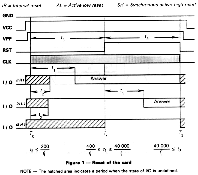
A card reset is initiated by the interface device, whereupon the card shall respond with an Answer-to-Reset as described in clause 6.
By the end of the activation of the contacts (RST in state L, VCC powered and stable, I/O in reception mode in the interface device, VPP stable at idle state, CLK provided with a suitable and stable clock), the card answering asynchronously is ready for reset. See figure 1.
The clock signal is applied to CLK at time T0. The I/O line shall be set to state Z within 200 clock cycles of the clock signal (t2) being applied to CLK (time t2 after T0).
An internally reset card is reset after a few cycles of the clock signal. The Answer-to-Reset on I/O shall begin between 400 and 40 000 clock cycles (t1) after the clock signal is applied to CLK (time t1 after T0).
A card with an active low reset is reset by maintaining RST in state L for at least 40 000 clock cycles (t3) after the clock signal is applied to CLK (time t3 after T0). Thus, if no Answer-to-Reset begins within 40 000 clock cycles (t3) with RST in state L, RST is put to state H (at time T1). The Answer-to-Reset on I/O shall begin between 400 and 40 000 clock cycles (t1) after the rising edge of the signal on RST (time t1 after T1).
If the Answer-to-Reset does not begin within 40 000 clock cycles (t3) with RST in state H (t3 after T1), the signal on RST shall be returned to state L (at time T2) and the contacts shall be deactivated by the interface device. See subclause 5.4.
With a card answering synchronously, the interface device sets all lines to state L. See figure 2. VCC is then powered, VPP is set to idle state, CLK and RST remain in state L, I/O is put in reception mode in the interface device. RST shall be maintained in state H for at least 50 µs (t12), before returning to state L again.
The clock pulse is applied after an interval (t10) from the rising edge of the reset signal. The duration for the state H of the clock pulse can be any value betwee 10 µs and 50 µs; no more than one clock pulse during reset high is allowed. The time interval between the falling edges on CLK and RST is t11.
5
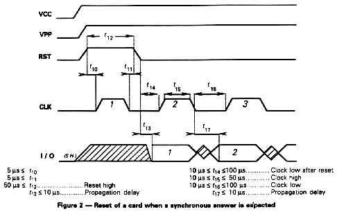
The first data bit is obtained as an answer on I/O while CLK is in state L and is valid after an interval t13 from the falling edge on RST.
NOTES
1 The internal state of the card is assumed not to be defined before reset. Therefore the design of the card has to avoid improper operation.
2 In order to continue the dialogue with the card, RST shall be maintained in the state where an answer occurs on I/O.
3 Reset of a card can be initiated by the interface device at its discretion at any time.
4 Interface devices may support one or more of these types of reset behaviour. The priority of testing for asynchronous or synchronous cards is not defined in this standard.
5.3 Answer-to-Reset and subsequent information exchange
The card answers after reset with a sequence defined in clause 6.
All data exchanged over the I/O circuit correspond to the execuion of commands (via RST for reset and via I/O for any other command).
As for Answer-to-Reset, the operating procedure of commands (except those commands to be specified in the next part of ISO/IEC 7816) depends on the type of transmission (asynchronous or synchronous) and on the protocol type.
NOTES
1 The asynchronous half duplex character transmission protocol, with the interface device as the master, is specified in clause 8, the asynchronous half duplex block transmission protocol in clause 9. Further protocol types between the card and the interface device are for further study.
2 The interindustry commands for interchange are to be specified in the next part of ISO/IEC 7816. Application specific commands are specified either in existing standards or in additional standards to be defined.
5.4 Deactivation of the contacts
When information exchange is terminated or aborted (unresponsive card or detection of card removal), the electrical contacts shall be deactivated.
The deactivation by the interface device shall consist of the consecutive operations:
-- State L on RST;-- State L on CLK;
-- VPP inactive;
-- State A on I/O;
-- VCC inactive.
6
Two types of transmission are considered
Asynchronous trsnsmission
In this type of transmission, characters are transmitted on the I/O line in an asynchronous half duplex mode Each character includes an 8-bit byte. See 6.1.2.
Synchronous transmission
In this type of transmission, a series of bits is transmitted on the I/O line in half duplex mode in synchronisation with the clock signal on CLK.
6.1 Answer-to-Reset in asynchronous transmission
6.1.1 Bit duration
The nominal bit duration used on I/O is defined as one Elementary Time Unit (etu).
For cards having internal clock, the initial etu is 1/9 600 s.
For cards using the external clock, there is a linear relationship between the Elementary Time Unit used on I/O and the period provided by the interface device on CLK.
The initial etu is 372/fi where fi is in hertz.See also 6.1.4.1.
The initial frequency fi is provided by the interface device on CLK during the answer to reset, as defined in 4.2.5.
In order to read the initial character (TS), all cards shall initially be operated with fi in the range of 1 MHz to 5 MHz.
6.1.2 Character frame during answer to reset
Prior to the transmission of a character, I/O shall be in state Z.
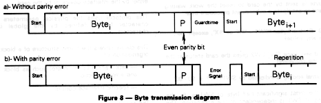
A character consists of ten consecutive bits: a start bit in state A, eight bits of information, designated ba to bh and conveying a data byte, and a tenth bit bi used for even parity checking.
A data byte consists of 8 bits designated bl to b8, from the least significant bit (lsb, b1 ) to the most significant bit (msb, b8).
Conventions (level coding, connecting levels Z/A to digits 1 or 0; and bit significance, connecting ba--bh to b1--b8) are specified in the initial character, called TS, which is transmitted by the card in response to reset.
Parity is correct when the number of ONES is even in the sequence from ba to bi.
Within a character, the time from the leading edge of the start bit to the trailing edge of the nth bit shall equal (n±0,2) etu.
When searching for a start, the receiver samples I/O periodically. The time origin being the mean between last observation of level Z and first observation of level A, the start shall be verified before 0,7 etu, and then ba is received at (1,5±0,2) etu, bb at (2,5±0,2) etu, ... bi at (9,5±0,2) etu. Parity is checked on the fly.
NOTE -- When searching for a start, the samciing time shall be less than 0,2 etu so that all the test zones are distinct from the transition zones.
The delay between two consecutive characters (between start leading edges) is at least 12 etu, including a character duration (10±0,2) etu plus a guardtime. While in guardtime, the interface device and the card remain both in reception, so that I/O is in state Z. See figure 3.
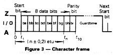
During the answer to reset, the delay between the start leading edges of two consecutive characters from the card shall not exceed 9 600 etu. This maximum value is named initial waiting time.
6.1.3 Error detection and character repetition
During the answer to reset, the following character repetition procedure depends on the protocol type. See 6.1.4.3. This procedure is mandatory for cards using the protocol type T=0; it is optional for the interface device and for other cards.
The transmitter tests I/O, (11±0,2) etu after the start leading edge:
-- If I/O is in state Z, the correct reception is assumed .-- If I/O is in state A, the transmission is assumed to have been incorrect. The disputed character shall be repeated after a delay of at least 2 etu after detection of the error signal.
When parity is incorrect, from (10,5±0,21 etu, the receiver transmits an error signal as state A for 1 etu minimum and 2 etu maximum. The receiver then shall expect a repetition of the disputed character. See figure 8.
If no character repetition is provided by the card,
-- the card ignores and shall not suffer damage from the error signal coming from the interface device;-- the interface device shall be able to initiate the repetition of the whole Answer-to-Reset sequence.
7
6.1.4 Structure and content
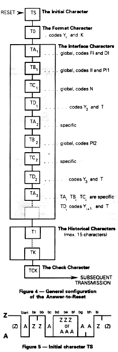
A reset operation results in an answer from the card consisting of the initial character TS, followed by at most 32 characters in the following order:
-- T0 ............... Format character ......... Mandatory-- TAi TBi TCi TDi .... Interface characters ...... Optional
-- T1 T2 ...TK ....... Historical characters ..... Optional
-- TCK .............. Check character ........ Conditional
See 6.1.4.1 to 6.1.4.4 and figure 4.
The interface characters specify physical parameters of the integrated circuit in the card and logical characteristics of the subsequent exchange protocol.
The historical characters designate general information, for example, the card manufacturer, the chip inserted in the card, the masked ROM in the chip, the state of the life of the card. The specification of the historical characters falls outside the scope of this part of ISO/IEC 7816.
For notational simplicity, T0 TAi ... T1 ... TCK will designate the bytes as well as the characters in which they are contained.
6.1.4.1 Structure of TS, the initial character
The initial character TS provides a bit synchronisation sequence and defines the conventions to code data bytes in all subsequent characters. These conventions refer to ISO 1177.
I/O is initially in state Z. A bit syncnronization sequence (Z)AZZA is defined for the start bit and bits ba bb bc. See figure 5.
The 3 bits bd be bf specify inverse or direct convention, with values of AAA or ZZZ, respectively.
The last 3 bits bg bh bi shall be AAZ for checking parity.
NOTE --This allows the interface device to determine the etu initially used by the card. An alternate measurement of etu is a third of the delay between the first two falling edges in TS. Transmission and reception mechanisms in the card (including the tolerances described in 6.1.2 and 6.1.3) shall be consistent with this alternate definition of etu.
The two possible values of TS (ten consecutive bits from start to bi and corresponding hexadecimal value) are
--Inverse convention: (Z)AZZAAAAAAZ where logic level ONE is A, ba is b8 (msb is first), equal to '3F' when decoded by inverse convention.
--Direct convention: (Z)AZZAZZZAAZ where logic level ONE is Z, ba is b1 (lsb is first), equal to '3B' when decoded by direct convention.
8
6.1.4.2 Structure of the subsequent characters in the Answer-to-Reset
The initial character TS is followed by a variable number of subsequent characters in the following order: the format character T0 and, optionally, the interface characters TAi TBi TCi TDi and the historical characters T1 T2 ... TK and, conditionally, the check character TCK.
The presence of the interface characters is indicated by a bit map technique explained below.
The presence of the historical characters is indicated by the number of bytes as specified in the format character defined below.
The presence of the check character TCK depends on the protocol type(s) as defined below.
Format character T0
The T0 character contains two parts:
-- The most significant half byte (b5 b6 b7 b8) is named Y1 and indicates with a logic level ONE the presence of subseauent interface characters TAi TBi TCi TDi respectively.-- The least significant half byte (b4 to bl) is named K and indicates the number (0 to 15) of historical characters. See figure 6.
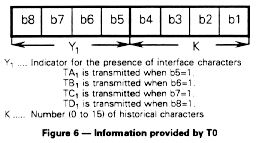
Interface characters TAi TBi TCi TDi
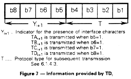
TAi TBi TCi (i = 1, 2, 3 ...) indicate the protocol parameters. TDi indicates the protocol type T, as defined in 6.1.4.3, and the presence of subsequent interface characters.
Bits b5 b6 b7 b8 of the byte containing Yi (T0 contains Y1; TDi contains Yi+1) state whether character TAijfor b5, character TBi for b6, character TCi for b7, character TDi for b8 are or are not (depending on whether the relevant bit is 1 or 0) transmitted subsequently in this order after the character containing Yi.
When needed, the interface device shall attribute a default value to information corresponding to a non transmitted interface character.
When TDi is not transmitted, the cefault value of Yi+1 is null, indicating that no further interface characters TAi+1 TBi+1 TCi+1 TDi+1 will be transmitted. See figure 7.
Historical characters T1 T2 ... TK
When K is not null, the Answer-to-Reset is continued by transmitting K historical characters T1 T2 ... TK
Check character TCK
The value of TCK shall be such that the exclusive-oring of all bytes from T0 to TCK included is null.
The Answer-to-Reset is complete 12 etu after the leading edge of the last character.
6.1.4.3 Protocol type T
The four least significant bits of any interface byte TDi indicate a protocol type T, specifying rules to be used to process transmission protocols. When TD1 is not transmitted, T=0 is used.
T = 0 is the asynchronous half duplex character transmission protocol specified in clause 8.
T = 1 is the asynchronous half duplex block transmission protocol specified in clause 9.
T = 2 and T = 3 are reserved for future full duplex operations.
T= 4 is reserved for an enhanced asynchronous half duplex character transmission protocol.
T = 5 to T = 13 are reserved for future use.
T = 14 is reserved for protocols not standardized by ISO.
T = 15 is reserved for future extension.
TA1 TB1 TC1 and TB2 are the global interface bytes specified in 6.1.4.4. These global interface bytes shall be interpreted in order to process any transmission protocol correctly.
9
The other interface bytes TAi TBi TCi are the specific interface bytes. Their interpretation aepends on the protocol type indicated by T in TDi+1.
If more than three interface bytes TAi TBi TCi are defined for a specific protocol type and are to be sent in the Answer-to-Reset sequence, they shall be sent subsequently by using TD-bytes which all indicate the same protocol type.
If more than one protocol type is indicated and T=0 is one of them, T=0 shall be indicated first.
If only T=0 is indicated, TCK shall not be sent. In all other cases, TCK shall be sent.
6.1.4.4 Specifications of the global interface bytes
Among the interface bytes possibly transmitted by the card in Answer-to-Reset, this subclause defines only the global interface bytes TA1 TB1 TC1 TB2.
These global interface bytes convey information to determine parameters which the interface device shall take into account.
Parameters F, D, I, P, N
The initial etu used during Answer-to-Reset is replaced by the work etu during subsequent transmissions. F is the clock rate conversion factor and D is the bit rate adjustment factor to determine the work etu in subseouent transmissions.
For internal clock cards:
Initial etu = 1/9 600 s Work etu = 1/D x 1/9 600 s
For external clock cards:
Initial etu = 372/fi s Work etu = 1/D x F/fi swhere fi and fs in hertz are defined in 4.2.5.
The minimum value of fs shall be 1 MHz.
The maximum value of fs is given by table 6.
FI |
0000 |
0001 |
0010 |
0011 |
0100 |
0101 |
0110 |
0111 |
F |
Internal Clock |
372 |
558 |
744 |
1116 |
1488 |
1860 |
RFU |
fs (max) MHz |
-- |
5 |
6 |
8 |
12 |
16 |
20 |
-- |
RFU = Reserved for Future Use
FI |
1000 |
1001 |
1010 |
1011 |
1100 |
1101 |
1110 |
1111 |
F |
RFU |
512 |
768 |
1024 |
1536 |
2048 |
RFU |
RFU |
fs (max) MHz |
-- |
5 |
7,5 |
10 |
15 |
20 |
-- |
-- |
I and P define the active state at VPP.
-- Maximum programming current: IPP = I mA.-- Proqramming voltage: VPP = P V.
N is an extra guardtime requested by the card. Before receiving the next character, the card requires a delay of at least (12+N) etu from the start leading edge of the previous character. No extra guardtime is used to send characters from the card to the interface device.
The default values of these parameters are
F = 372: D = 1; I = 50; P = 5; N = 0.
These parameters are described in greater detail at the end of this subclause under Integer Values to Parameters Correspondence.
Integer values in the global interface bytes
The global interface bytes TA1 TB1 TC1 TB2 code integer values FI, DI, II, PI1, N, PI2 which are either equal to or used to compute the values of the parameters F, D, I, P, N presented above.
TA1 codes FI over the most significant half byte (b8 to b5), and DI over the least significant half byte (b4 to b1). See tables 6 and 7.
TB1 codes ll over the bits b7 and b6, and PI1 over the 5 least significant bits b5 to b1. See table 8. The most significant bit b8 equals 0.
NOTE -- The interface device may ignore the bit b8 of TB1.
TC1 codes N over the eight bits (b8 to b1).
TB2 codes Pl2 over the eight bits (b8 to b1).
All undefined values of the following parameters are reserved for future use by ISO/IEC JTC1/SC17.
Integer values to parameters correpondence
The correspondence between the parameters F, D, I, P, N and the integer values FI, DI, II, PI1, N, PI2 is given below.
10
DI |
0000 |
0001 |
0010 |
0011 |
0100 |
0101 |
0110 |
0111 |
D |
RFU |
1 |
2 |
4 |
8 |
16 |
RFU |
RFU |
DI |
1000 |
1001 |
1010 |
1011 |
1100 |
1101 |
1110 |
1111 |
D |
RFU |
RFU |
1/2 |
1/4 |
1/8 |
1/16 |
1/32 |
1/64 |
Programming voltage factor P
PI1 from 5 to 25 gives the value of P in volts. PI1=0 indicates that VPP is not connected in the card which generates an internal programming voltage from VCC. Other values of PI1 are reserved for future use.
When PI2 is present, the indication of PI1 should be ignored. PI2 from 50 to 250 gives the value of P in 0,1 V. Other values of PI2 are reserved for future use.
II |
00 |
01 |
10 |
11 |
I |
25 |
50 |
100 |
RFU |
Extra guardtime N
N codes directly the extra guardtime, from 0 to 254 etu. N=255 indicates
that the minimum delay between the start leading edges of two consecutive
characters is reduced to 11 etu.
6.2 Answer-to-Reset in synchronous transmission
6.2.1 Clock frequency and bit rate
There is a linear relationship between the bit rate on the I/O line and the clock frequency provided by the interface device on CLK
Any clock frequency between 7 kHz and 50 kHz may be chosen for the reset sequence. A clock frequency of 7 kHz corresponds to 7 kbit/s, and values of the clock frequency up to 50 kHz cause corresponding bit rates to be transmitted .
6.2.2 Structure of the header of Answer-to-Reset
The reset operation results in an answer from the card containing a header transmitted from the card to the interface. The header has a fixed length of 32 bits and beains with two mandatory fields of 8 bits, H1 and H2
The chronological order of transmission of the information bits shall correspond to bit identification b1 to b32 with the least significant bit transmitted first. The numerical meaning corresponding to each information bit considered in isolation is that of the digit
-- 0 for a unit corresponding to state A (space);-- 1 for a unit corresponding to state Z (mark).
6.2.3 Timing of the header
After the reset procedure, see 5.2 and figure 2, the output information is controlled by clock pulses. The first clock pulse is applied between 10 µs and 100 µs (t14) after the falling edge on RST to read the data bits from the card. State H of clock pulses can be varied between 10 µs and 50 µs (t15) and state L between 10 µs and 100 µs (t16).
The first data bit is obtained on I/O while the clock is low and is valid 10 µs (t13) at least after the falling edge on RST. The following data bits are valid 10 µs (t17) at least after the falling edge on CLK. Each data bit is valid until the next falling edge of the following clock pulse on CLK. The data bits can therefore be sampled at the rising edge of the following clock pulses.
6.2.4 Data content of the header
The header allows a quick determination of whether the card and the interface device are compatible. If there is no compatibility, the contacts shall be deactivated according to subclause 5.4.
The first field H1 codes the protocol type. The values of the codes and the corresponding protocol types are
Hexadecimal value Protocol type '00' and 'FF' not to be used '01' to 'FE' each value is assigned by ISO/IEC JTC1tSC17 to one protocol type.
The second field H2 codes parameters for the protocol type coded in field H1. The values of H2 are to be assigned by ISO/IEC JTC1/SC17.
The specifications of the remaining fields fall outside the scope of this part of ISO/IEC 7816. The role of these remaining fields is similar to that of the historical characters mentioned in 6.1.4.
11
If only one protocol type and FI=D=1 (default value of TA1) and N smaller than 255 is indicated in the Answer-to-Reset, the transmission protocol associated to the protocol type may be started immediately after the transmission of the Answer-to-Reset.
If more than one protocol type and/or TA1 parameter values other than the default values and/or N equal to 255 is/are indicated in the Answer-to-Reset, the card shall know unambiguously, after having sent the Answer-toReset, which protocol type and/or transmission parameter values (FI, D, N) will be used. Consequently a selection of the protocol type and/or the transmission parameter values shall be specified.
If the card is able to process more than one protocol type and if one of those protocol types is indicated as T=0 then the protocol type T=0 shall be indicated in TD1 as the first offered protocol, and is assumed if no PTS is performed
If a card offers more than one protocol and if the interface device supports only one of these protocols which is not T=0 and does not support PTS, the interface device should reject or reset the card.
7.1 PTS protocol
Only the interface device is permitted to start the PTS procedure:
-- The interface device sends a PTS request to the card.-- If the card receives a correct PTS request, it answers by sending a PTS confirm, if implemented, or the initial waiting time will be exceeded.
-- After the successful exchange of PTS request and PTS confirm, data shall be transmitted from the interface device to the card using the selected protocol type and/or transmission parameters.
-- If the card receives an erroneous PTS request, it will not send a PTS confirm.
-- If the initial waiting time is exceeded, the interface device should reset or reject the card.
-- If the interface device receives an erroneous PTS confirm, it should reset or reject the card.
The parameters for the transmission of the PTS request and PTS confirm shall correspond to those used within the Answer-to-Reset regarding the bit rate and the convention detected by TS and possibly modified by TC1 (extra guardtime).
7.2 Structure and content of PTS request and PTS confirm
The PTS request and PTS response each consist of one initial character PTSS, followed by a format character PTS0, three optional parameter characters PTS1 PTS2 PTS3, and a character check PCK as the last byte.
PTSS identifies the PTS request or PTS confirm and is coded 'FF' .
PTS0 indicates by the bits b5, b6, b7 set to 1 the presence of the subsequently sent optional characters PTS1, PTS2, PTS3, respectively. It codes over the least significant bits b4 to b1 the selected protocol type T as coded in TD-bytes. The most significant bit b8 (default : b8=0) is reserved for future use.
PTS1 codes the parameter values FI and D as coded in TA1. The interface device may send PTS1 in order to indicate the selected FI and/or D values to the card. If PTS1 is not sent, FI=1 and D=1 are assumed as defaults. The card either acknowledges both the FI and D values by echoing PTS1 or does not send PTS1 indicating the use of the default values.
PTS2 indicates the support of N=255, when bit b1 is set to 1. Bit b1 set to 0 is the default and indicates that the 11-etu period is not used. If bit b2 is set to 1, the card shall use an extra guardtime of 12 etu for its transmission of characters to the interface device Bit b2 set to 0 is the default and indicates that no extra guardtime is required. Bits b3 to b8 are reserved for future use.
If PTS2 is sent by the interface device and is not echoed by the card, the interface device should reject or reset the card .
The coding and use of PTS3 is to be defined.
The value of PCK shall be such that the exclusive-oring of all characters
from PTSS to PCK included is null.
This clause defines the structure and processing of commands initiated by an interface device for transmission control and for card specific control in an asynchronous half duplex character transmission protocol .
This protocol uses the parameters indicated by the Answer-to-Reset, unless modified by protocol type selection.
Interindustry commands for international interchange will be defined in the next part of ISO/IEC 7816.
12
8.1 Specific interface parameter : the work waiting time
ln the Answer-to-Reset, the interface character TC2 codes the integer value WI over eight bits b8 to b1. When no TC2 appears in the Answer-to-Reset, the default value of WI is 10.
The interval between the start leading edge of any character sent by the card and the start leading edge of the previous character (sent either by the card or by the interface device) shall not exceed 960 x D x WI work etu. This maximum delay is named the work waiting time.
8.2 Structure and processing commands
A command is always initiated by the interface device. It tells the card what to do in a 5-byte header, and allows a transfer of data bytes under control of procedure bytes sent by the card.
It is assumed that the card and the interface device know a priori the direction of data, in order to distinguish between instructions for incoming data transfers (where data enter the card during execution) and instructions for outgoing data transfers (where data leave the card during execution).
During transmission by the card or the interface device, the error detection and character repetition procedure described in 6.1.3 is mandatory. See figure 8.
8.2.1 Command header sent by the interface device
The interface device transmits a header over five successive bytes designated CLA, INS, P1, P2, P3.
-- CLA is an instruction class. The value 'FF' is reserved for PTS. See clause 7.-- INS is an instruction code in the instruction class. The instruction code is valid only if the least significant bit is 0, and the most significant half byte is neither '6' nor '9'.
-- P1 P2 are a reference (e.g. an aadress) completing the instruction code.
-- P3 codes the number n of da-a bytes (D1...Dn) which are to be transmitted during the command. The direction of movement of these data is a function of the instruction. In an outgoing data transfer command, P3=0 introduces a 256-byte data transfer from the card. In an ingoing data transfer command, P3=0 introduces no transfer of data.
All remaining encoding possibilities for the header are specified in subsequent parts of ISO/IEC 7816.
After transmission of such a 5-byte header, the interface device waits for a procedure byte.
8.2.2 Procedure byte sent by the card
The values of the procedure bytes shall indicate the action requested by the interface device. Three types of procedure bytes are specified:
-- ACK (the seven most significant bits in an ACK byte are all equal or all complementary to those in the INS byte, apart from the values '6X' and '9X'). The interface device controls VPP state and exchanges data depending on ACK values-- NULL (= '60'). This byte is sent by the card to restart the work waiting time, and to anticipate a subsequent procedure byte. It requests no further action neither on VPP nor on data.
-- SW1 (= '6X' or '9X', except '60'). The interface device maintains or sets VPP at idle and waits for a SW2 byte to complete the command.
Any transition of VPP state (active/idle) must occur within the guardtime of the procedure byte, or on the work waiting time overflow
At each procedure byte, the card can proceed with the command by an ACK or NULL byte, or show its disapproval by becoming unresponsive, or conclude by an end sequence SW1-SW2. See table 9.
13
Byte |
Value |
Result |
ACK |
INS |
VPP is idle. All remaining data bytes are transferred subsequently. |
INS + 1 |
VPP is active. All remaining data bytes are transferred subsequently. |
|
____ |
VPP is idle. Next data byte is transferred subsequently. |
|
________ |
VPP is active. Next data byte is transferred subsequently. |
|
NULL |
'60' |
No further action on VPP. The interface device waits for a new procedure byte. |
SW1 |
SW1 |
VPP is idle. The interface device waits for a SW2 byte. |
8.2.2.1 Acknowledge bytes
The ACK bytes are used to control VPP state and data transfer.
-- When exclusive-oring the ACK byte with the INS byte gives '00' or 'FF', the interface device maintains or sets VPP at idle.-- When exclusive-oring the ACK byte with the INS byte gives '01' or 'FE', the interface device maintains or sets VPP at active.
-- When the seven most significant bits in the ACK byte have the same value as those in the INS byte, all remaining data bytes (Di...Dn), if any remain, are transferred subsequently.
-- When the seven most significant bits in the ACK byte are complementary to those in the INS byte, only the next data byte (Di), if one remains, is transferred.
After these actions, the interface device waits for a new procedure byte.
8.2.2.2 Null byte (= '60')
This byte is sent by the card to reset the work waiting time and to anticipate a subsequent procedure byte.
8.2.2.3 Status bytes (SW1 = '6X' or '9X', except '60'; SW2 = any value)
The end sequence SW1-SW2 gives the card status at the end of the command.
The normal ending is indicated by SW1-SW2 = '90'-'00'.
When the most significant half byte of SW1 is '6', the meaning of SW1 is independent of the application. The following five values are defined:
'6E' The card does not support the instruction class.'6D' The instruction code is not programmed or is invalid.
'6B' The reference is incorrect.
'67' The length is incorrect.
'6F' No precise diagnosis is given.
Other values are reserved for future use by ISO/IEC JTC1/SC17.
When SW1 is neither '6E' nor '6D', the card supports the instruction.
This part of ISO/IEC 7816 interprets neither '9X' SW1 bytes, nor SW2 bytes;
their meaning relates to the application itself
This transmission protocol is defined as the protocol type T=1 in a TDi-byte of the Answer-to-Reset.
This clause defines the structure and processing of commands for transmission control and for card specific control in an asynchronous half duplex block transmission protocol. These commands are initiated either by the interface device or by the card.
This protocol uses the physical parameters and the character frame defined by the global interface characters .
This clause covers the frame structure of a block and the orqanisation of
-- data transmission control such as block chaining and error correction,
-- specific interface control.
The specification of this protocol is under study and will be included in this clause when available.
14
[Blank page]
UDC 351.755.62 : 3-049.77
Descriptors: data processing, identity cards, intearated circuits, data transmission, communication procedure.
Price based on 14 pages
[End intitial section of Part 3]
Related documents in (slow) preparation:
Part 3 Amendment 1: Protocol type T = 1, asynchronous half duplex block transmission protocol, 13 pp.
Part 3 Amendment 2: Revision of protocol selection, 8 pp.
ISO/IEC 7816-4 Part 4: Interindustry commands for interchange, 46 pp.